|
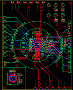
 Printed Circuit Board (PCB) layout engineering and the supporting engineering of schematic capture are the core areas for Nimbeon's service offerings. Nimbeon has the tools and knowledge to design your board no matter how large or small. Every PCB design that Nimbeon provides is a custom PCB, unique to our specific customers. Again, the below capabilities are only a partial list .We use the industries top tier design tools and are driven to be the best. Printed Circuit Board (PCB) layout engineering and the supporting engineering of schematic capture are the core areas for Nimbeon's service offerings. Nimbeon has the tools and knowledge to design your board no matter how large or small. Every PCB design that Nimbeon provides is a custom PCB, unique to our specific customers. Again, the below capabilities are only a partial list .We use the industries top tier design tools and are driven to be the best.
The applications we have serviced cover a wide range of functionality including:
- Digital signal processing
- Analog and mixed signal applications.
- High frequency products (>10GHz) &RF at 2.4GHz.
- Impedance control PCB's AC/DC and DC/DC converters.
- HDI Designs with micro vias and advanced materials - Via-in-Pad, laser micro vias.
- High speed, multi layer digital PCB designs - Bus routing, differential pairs, matched lengths.
- PCB Designs for Semiconductor, R&D labs, Telecommunications, military, medical and commercial applications.
- DDR, DDR2, DDR3, SAS and differential pair routing expertise
- High density SMT designs (BGA, uBGA, PCI, PCIE, CPCI...)
- Flex PCB designs of all types
- Low level analog PCB designs for metering
- Ultra low EMI designs for MRI applications
Nimbeon has invested in many suites of EDA tools to complete both schematic capture and PCB layout engineering. Every project uses these EDA tools but at Nimbeon the actual layout is completed with 100% manual routing. In addition to the 100% manual routing used by Nimbeon, we use an indigenously developed quality assurance system, which allows us to guarantee that the final layout will exactly reproduce the schematic. A customer may require many other features or performance criteria that require engineering efforts.
A partial list of some of these engineering issues that Nimbeon can address is:
- Design For Manufacturing (DFM) Capabilities
- Support of Length, Parallelism & Differential Pairs
- Complex Physical Design Rule Checking (DRC)
- Parasitic Measurement & Split Planes Designs
- Assembly DRC , Support of Skill Runtime, Macro & Script
- Support of Min/Max & Matched Length
- Crosstalk Controls (same and adjacent layers)
- Length & Gap Control of Parallelism
- Design of Differential Pairs, Net Shielding & EMI Suppression
- Test data generation
- Extensive RF and analog design experience (printed antennas, guard rings, RF shields...)
- Signal integrity issues to meet your digital design needs (tuned traces, diff pairs...)
|